Geometry
Shape
Thickness, TTV (GBIR), Bow, Warp, GFLR. An upper and a lower capacitive probe face each other across the wafer and read it without contact.
Semiconductor Wafer Metrology & Sorting
ZILAB builds the ZAFS series — systems that measure the thickness, flatness, resistivity, polarity and ID of a silicon wafer in a single handling pass, then sort it by grade. At the 0.01 µm scale, accuracy is not decided by the sensor reading. It is decided by how honestly you model the physics acting on the wafer.
What we build
Moving wafers between separate tools costs time and adds scatter. ZAFS takes everything it needs from one pick-up — geometry, electrical properties and identity — and routes each wafer to the output port its recipe assigns.
Geometry
Thickness, TTV (GBIR), Bow, Warp, GFLR. An upper and a lower capacitive probe face each other across the wafer and read it without contact.
Electrical
Resistivity from 1 to 1,000 Ω·cm and P/N polarity. Resistivity can be probed at up to three points per wafer to show the distribution across it.
Identity
Two OCR units read the laser-marked ID on the front and back side and check it against the cassette barcode. Diameter is verified, then the wafer is sorted into its grade port.
Scientific originality
Two tools with the same sensor report different numbers. The difference lies in how each one handles the physics the wafer experiences while it is being measured. These are the four problems ZILAB set up differently.
A silicon disc 300 mm across and 0.8 mm thick sags by several micrometres under its own weight alone. What a wafer on a chuck shows you is always its own shape plus the elastic sag caused by gravity. ZILAB sets this up as a plate-deflection problem derived from the elastic constants of silicon and the support conditions, calibrates the coefficients against a reference wafer, and subtracts it from the measurement.
This is not an empirical offset. Because the term comes out of a physical equation, it can be rebuilt by the same reasoning when wafer thickness or support conditions change.
The two probes face each other across the wafer. Because the reference gap between them is fixed, subtracting the sum of the two distances from that gap gives thickness without ever flipping the wafer, while the difference between them gives the position of the neutral plane — the shape.
No separate thickness run and shape run. Both values come from the same sampled instant, so the error a time gap would introduce simply does not exist.
The theta axis rotates the wafer 120° between passes, scanning three diameters at 2 mm pitch. All three lines cross at the centre, so they constrain each reference plane against the others. That constraint lets us derive a least-squares (Best-fit) and a 3-Point reference plane from the same data.
Whichever definition your specification uses, no re-measurement is needed. The number of scan lines can be increased in the recipe.
Hunting for the apex of the notch turns sensor noise directly into angular error. ZILAB instead estimates the apex as the midpoint between where the notch enters the sensor window and where it leaves. Using the symmetry of the notch profile makes the estimate insensitive to noise.
After the change, the scatter of the angle estimate fell by more than an order of magnitude. A stable alignment keeps the centre where the three lines meet stable as well.
Verification
A metrology tool cannot prove its own numbers. ZILAB measures the same wafers alongside a comparable commercial tool already running on the production floor, and checks directly against reference wafers whose values the customer has fixed.
| Parameter | Reference | ZAFS | Delta |
|---|---|---|---|
| Warp (Best-fit) | 11.78 | 11.42 | 0.36 |
| Warp (3-Point) | 12.90 | 13.28 | 0.38 |
| Bow (Best-fit) | −5.16 | −5.35 | 0.20 |
| Bow (3-Point) | −8.47 | −8.58 | 0.12 |
ZAFS series
The measurement unit is the same. Wafer size, port count and the sorting function differ.
8 port · measure + sort
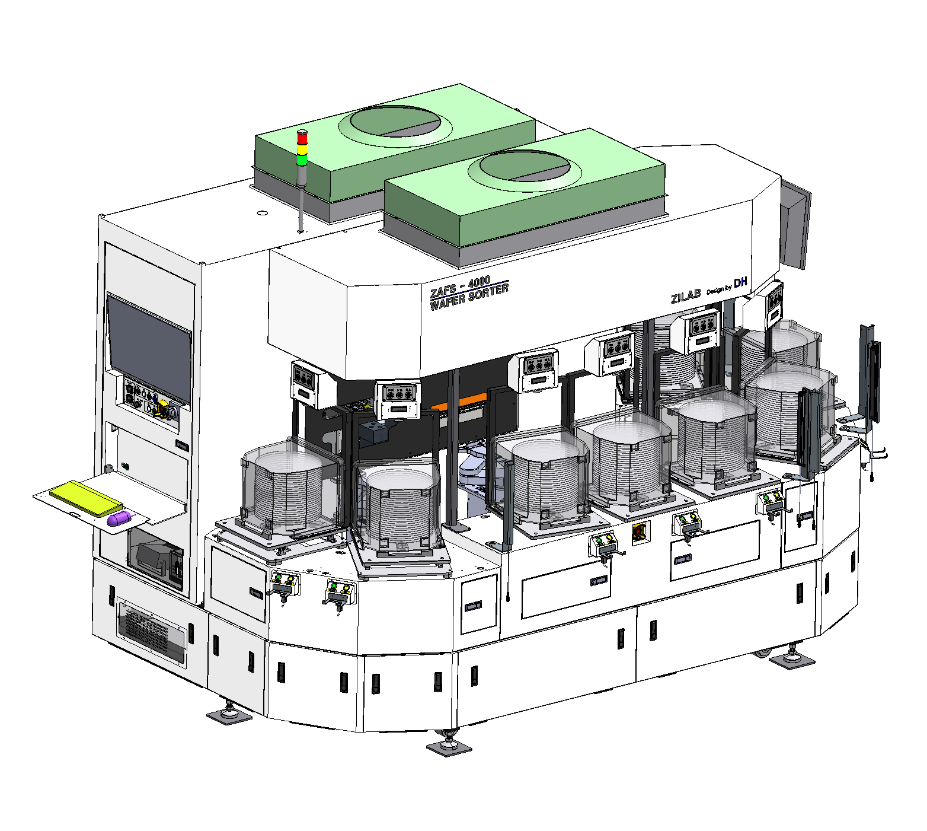
Measures every parameter on 300 mm and 200 mm wafers and sorts them by grade. Two input ports, six output ports (Grade 1 ×2, Grade 2 ×2, Reject ×2). 55 sec/wafer.
3 port · measurement only
The 3000 handles 300 mm wafers, the 2000 handles 200 mm. Same parameters and same measurement principle as the 4000, in a smaller footprint.
Where we are going
ZAFS already records the raw scan waveform, alignment diagnostics and motion history for every single wafer. Until now that record was something an engineer opened after a failure. From here it becomes the material for reading a failure before it happens.
Stage 1
Alignment failures and transfer stops do not arrive without warning. Leading indicators start to drift tens of minutes earlier. Learning them turns an unplanned stop into a planned one.
Stage 2
The learned model takes only the residual the physical models — gravity sag, stage reference plane — leave behind. A structure that does not collapse when data is scarce.
Stage 3 · 4
Dozens of parameters such as scan acceleration and alignment window are searched automatically from measured data, and automated regression on the simulator shortens the release cycle.
Patent
ZILAB has filed a patent application covering the core of the measurement principles described here, and it is currently under examination. The specific construction and claims will be published here once the application is laid open.
Company
ZILAB develops semiconductor metrology and inspection equipment. Engineers with 15 to 25 years in equipment development, and doctorates in robotics, vision and pattern recognition, build everything from the mechanical design to the control software in house.
Let physics carry what physics explains.
Give the data only what is left.
ZILAB Co., Ltd. founded
ZAFS series development begins
ZAFS 2000 (8″) shipped
wafer reclaim specialist
ZAFS 3000 (12″) shipped
major Korean wafer manufacturer
ZAFS 4000 unit #1 shipped
with sorting
ZAFS 4000 unit #2 shipped