ZILAB ZILAB Co., Ltd.

Technology

At the micrometre scale, the act of measuring changes the value

Gravity bends the wafer the instant it lands on the chuck. Floor vibration shakes the probe. A small alignment error puts the scan directions out of register with each other. The difficulty of a flatness metrology tool is not the resolution of its sensor — it is how honestly it separates out these disturbances. This page explains how ZILAB does that separation.

Measurement chain

The path one wafer takes

This is not an arbitrary outline. It is the sequence the tool actually performs on every wafer, and each step sets up the premise for the next one.

  1. STEP 1

    Mapping — pick up only what is there

    When a cassette arrives, the mapping sensor on the transfer robot reads the presence of a wafer in every slot in one pass. Empty slots are skipped, so the time once spent reaching into each slot disappears.

  2. STEP 2

    Alignment — bring the notch to the reference angle

    The aligner rotates the wafer while reading its edge, derives the centre offset (x, y) and the notch angle, and brings it to the reference angle set in the recipe. Every coordinate after this takes that angle as its origin.

    An alignment error is never recovered downstream. If the scan directions do not meet at the centre, the reference plane itself is wrong.

  3. STEP 3

    First scan — a linear motor passes at constant velocity

    The wafer travels between the facing capacitive probes. The scan axis is a linear motor, so there is no gear or belt backlash, and sampling happens in the constant-velocity region after acceleration has finished, at 2 mm pitch along R.

  4. STEP 4

    Rotate, then scan again — for every remaining line

    The theta axis turns the wafer and sends it through again, repeated as many times as the recipe specifies. The default configuration is 4 lines. The scan axis is fixed and the wafer is what rotates, so the geometry of the scan path itself is identical on every pass.

    Use a different axis per line and the geometric error between axes disguises itself as a line-to-line difference. Use the same axis every time and that error becomes a common term that cancels in the reference-plane calculation.

  5. STEP 5

    Electrical properties and ID

    Resistivity is probed at up to three points per wafer to show its distribution, and P/N polarity is determined. The theta axis turns the wafer to a set angle so the front and back OCR units can read the laser-marked ID, and diameter is checked.

  6. STEP 6

    Correction — gravity, stage, tool matching

    The gravity-sag component and the stage reference-plane component are removed from the raw waveform in turn, and coefficients from master-wafer calibration bring the tool into line with other units. Only here is the shape that belongs to the wafer left standing.

  7. STEP 7

    Reference planes and sorting

    From the remaining shape, Best-fit and 3-Point reference planes are derived and Thickness, TTV (GBIR), Bow, Warp and GFLR are computed. The result is checked against the grade conditions in the recipe and the sorting robot places the wafer in the matching output port.

The physics

Four problems we set up differently

None of these came from swapping in a better component. They came from framing the problem another way.

Gravity sag

Deriving the sag, then subtracting it

A silicon disc 300 mm across and 0.8 mm thick sags by several micrometres under its own weight. What a wafer on a chuck shows is always its own shape plus the elastic sag caused by gravity. Where the Warp specification is measured in tens of micrometres, that term is not something you can wave away.

ZILAB sets it up as a plate-deflection problem derived from the elastic constants of silicon and the support conditions, calibrates the coefficients against a reference wafer, and separates it from the measurement. Not a single offset value but a term with a shape that varies with radial position.

Because it comes out of a physical equation, it can be rebuilt by the same reasoning when wafer thickness or support conditions change. An empirical constant cannot be.

Dual capacitive probe

Thickness and shape at the same instant

The upper and lower capacitive probes face each other across the wafer. The reference gap G between them is fixed, so for an upper distance a and a lower distance b:

thickness = G − (a + b)
neutral plane = (a − b) / 2

Thickness comes out without ever flipping the wafer, and shape comes from the same sampled instant. The error a time gap between two runs would introduce simply does not exist. Being non-contact, the measurement never touches the wafer surface either.

Multi-line constraint

Several directions constrain one another

The theta axis turns the wafer between passes to scan several diameters. The default configuration is 4 lines — 0 / 45 / 90 / 135° in the wafer frame. All of them cross the centre, which imposes the constraint that the height at the centre must agree. That constraint reduces the freedom of each line reference plane — and works in reverse as a check on how well the alignment held.

A least-squares (Best-fit) and a 3-Point reference plane are derived from the same data, so no re-measurement is needed whichever definition your specification uses. The number of scan lines is selectable in the recipe — three or more.

Notch estimation

Symmetry instead of the apex

Hunting for the apex of the notch puts all the sensor noise carried by that one point straight into the angle. The notch is shallow and the edge curvature is large, so the signal flattens out exactly where the apex is — the worst place to be looking for a peak.

ZILAB estimates the apex as the midpoint between where the notch enters the sensor window and where it leaves. Because the method uses the symmetry of the notch profile, the noise on each of the two points averages out. After the change the scatter of the angle estimate fell by more than an order of magnitude.
Mechanical design

What computation cannot remove, structure has to block

Correction does not cover everything. Disturbances that do not repeat — floor vibration, reaction forces from the transfer section, thermal distortion of the frame — cannot be computed away. The right answer is to stop them reaching the measurement unit in the first place.

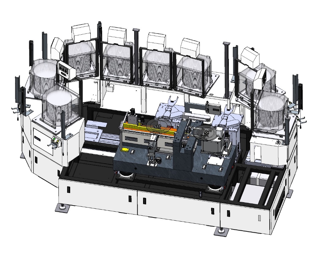
  • Measurement unit on granite — mass and stiffness suppress high-frequency distortion.
  • Air-spring vibration isolator — the whole granite base floats clear of the floor.
  • Linear-motor scan axis — no gears or belts, so no backlash and no transmitted vibration.
  • Non-contact measurement — the act of measuring applies no force to the wafer.
  • Top cover and area sensors on every port — dust ingress and operator interference are blocked.
Isometric drawing of the ZAFS 4000 interior — measurement unit on the central granite base with the linear scan stage, transfer robots either side, cassette ports around the perimeter
Interior — measurement unit on granite / linear scan stage / two transfer robots

Verification data

We would rather match than claim

A metrology tool cannot prove its own numbers. These are the three comparisons ZILAB runs before every shipment.

Repeatability — same point, 10 readings × 5 sets
Set12345
Mean (µm)832.23832.23832.24832.24832.23
Max − Min (µm)0.010.010.010.010.01
Std. dev. (µm)0.0020.0030.0020.0030.002

The thickness repeatability specification is ± 0.05 µm. The measured standard deviation sits more than an order of magnitude below it. (For Warp and Bow the specification is ± 0.5 µm.)

Reference wafer — Warp / Bow (mean of 7, µm)
ParameterReferenceZAFSDelta
Warp (Best-fit)11.7811.420.36
Warp (3-Point)12.9013.280.38
Bow (Best-fit)−5.16−5.350.20
Bow (3-Point)−8.47−8.580.12
Reference wafer — centre thickness / TTV (µm)
SlotThk. ref.Thk. meas.TTV error
1831.99832.17−0.10
2831.98832.06−0.15
3832.98833.07−0.05
4832.97832.99−0.13
5832.18832.20−0.13

Cross-measurement against a comparable commercial tool

The same seven MSA master wafers were measured side by side with a comparable commercial flatness tool already in production use. Warp, Bow and centre thickness all agreed slot by slot, and the differences stayed inside the deviation band established by the reference wafer comparison.

Acceptance Shipment requires zero tool-attributable errors across 100+ wafers of continuous auto running.

Software

We write the control software ourselves

Motion, transfer, measurement, correction maths, recipes, sorting decisions, logging and host integration are built by one team. The people who understand the measurement principle write the control code, so nothing is lost in translation between the physical model and its implementation.

  • A simulation layer that runs the whole process without hardware — new functions are exercised hundreds of times before they reach a real tool.
  • Raw data kept per wafer — scan waveform, alignment diagnostics and motion history are stored together, so any case can be reproduced afterwards.
  • Host integration — results are written directly into the customer MES or database.
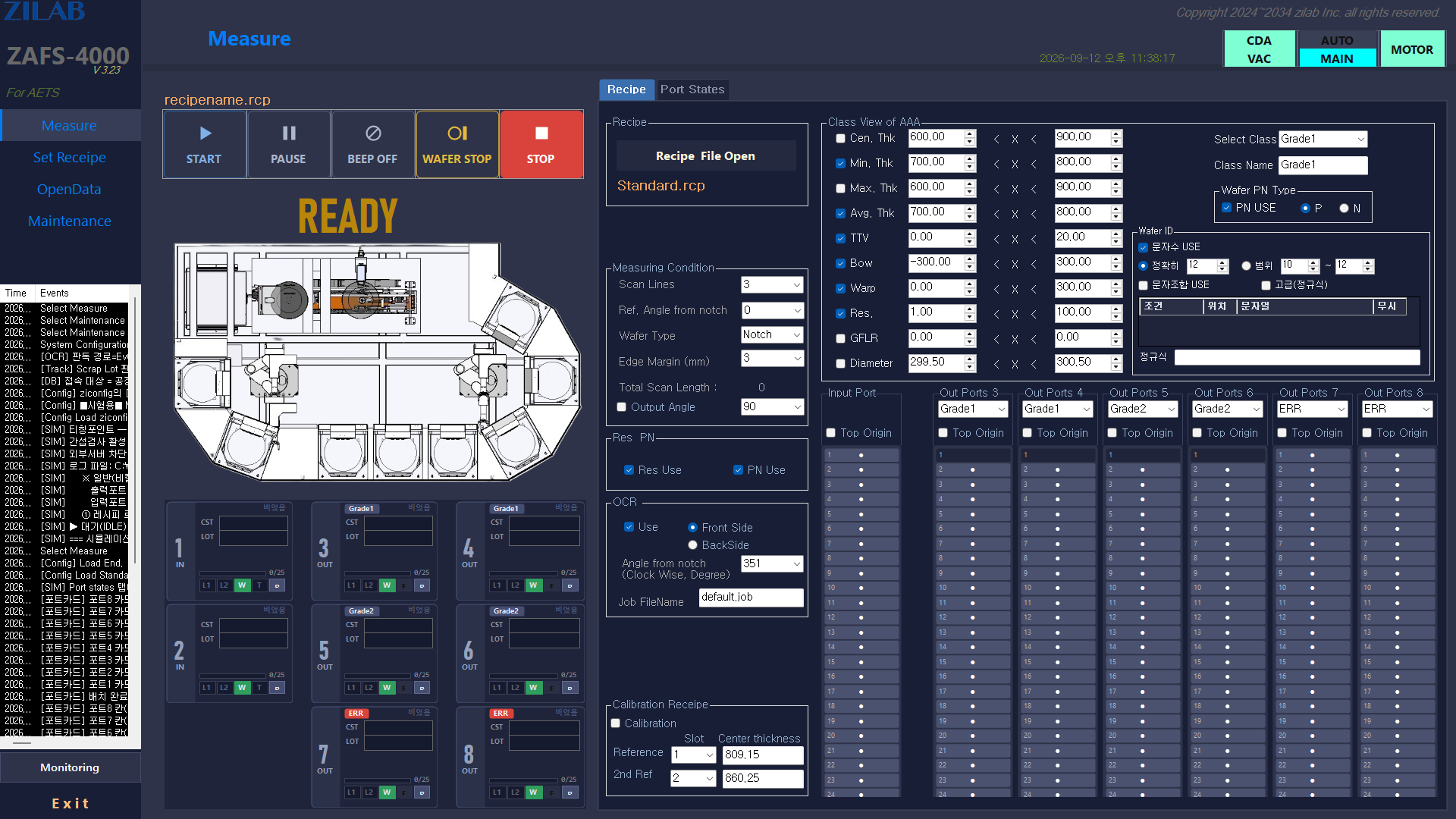
  • Recipe-driven operation — grade conditions, number of scan lines, resistivity probe points and OCR character count are all set in the recipe.
Measure screen of the ZAFS 4000 control software — tool layout and port status on the left, recipe and grade conditions on the right
Operating screen — port status and grade conditions on one screen

Patent

Patent pending

ZILAB has filed a patent application covering the core of the measurement principles described on this page, and it is currently under examination. The specific construction and claims will be published here once the application is laid open.

For technical discussions, material can be provided under a non-disclosure agreement. Get in touch